New Female Voice: Vernacular Newspapers in the Late Qing Dynasty and the Germination of Modern Female Consciousness
The female subject in the late Qing Dynasty and the early Republic of China gradually approached the "historical surface" through female text expression, and female expression, as a part of literary Chinese practice, experienced ups and downs with the transformation of modern literary Chinese. On the one hand, the changes of vocabulary, grammar and composition concepts provide key clues for the change of women’s concepts and text expression; On the other hand, women’s literary practice and discourse style in the transformation of Chinese, as the object of enlightenment, not only echo the changes of literary Chinese, but also reflect the process of self-adjustment of gender subjects in the nation and language. Borrowing Professor Wen Guiliang’s definition, the so-called "literary Chinese", that is, a connection between literature and language, brings the interaction and evolution between ancient Chinese and modern Chinese, classical Chinese and vernacular Chinese, classical Chinese and vernacular Chinese into the interpretation of literature in the late Qing Dynasty and the early Republic of China. Compared with traditional boudoir singing and vernacular writing after the May 4th Movement, women’s writing in this period conveyed not only radical determination, but also a dilemma. The vernacular newspaper is a window to examine China’s female consciousness and gender writing in the transitional period.
As a cadre of the May 4th Vernacular Movement, Hu Shi tried his best to separate the May 4th Vernacular Movement from the late Qing Dynasty Vernacular Movement, but he also recalled his experience of editing the late Qing vernacular newspaper Jingye Xunbao more than once. "In 1906, several of my classmates in China College ran a regular publication called Jingye Xunbao, another example of Darwin’s theory." I started writing in vernacular Chinese six years before the Republic of China (Bingwu). At that time, I wrote half a chapter novel and some papers for Shanghai Jingye Xunbao, all of which were written in vernacular Chinese. The "half-chapter novel" mentioned by Hu Shi is as true as an island written in vernacular, which already contains the content of criticizing early marriage. According to Chen Wanxiong’s statistics, there were 149 kinds of vernacular newspapers in the last decade of the late Qing Dynasty, not including the illustrated newspaper and some newspapers with both literary and vernacular styles. According to Cai Lesu’s textual research, there were more than 170 kinds of vernacular newspapers and periodicals in the late Qing Dynasty and the early Republic of China. On the basis of previous research, Professor Hu Quanzhang concluded that there were 257 kinds of vernacular newspapers founded in the last decade of the late Qing Dynasty. Among these huge late Qing newspapers and periodicals, Hu Shi’s example is just a drop in the ocean. These newspapers connected scholars from all over the world, trying to contribute their own strength to the cause of saving the nation and surviving, and then formed a massive vernacular movement in the late Qing Dynasty. A large number of vernacular newspapers in the late Qing Dynasty were founded in the name of region.Wuxi Vernacular Newspaper, Ningbo Vernacular Newspaper, Hangzhou Vernacular Newspaper, Wuhu Vernacular Newspaper, Hunan Vernacular Newspaper, Hubei Vernacular Newspaper, Jiangxi Vernacular Newspaper, Shanxi Vernacular Newspaper, Guangzhou Vernacular Newspaper, Fujian Vernacular Newspaper, Dianhua Daily, Tianjin Vernacular Newspaper, Hebei Vernacular Newspaper, Henan Vernacular Speech Newspaper and Shandong Vernacular Newspaper Although some vernacular newspapers were founded abroad, such as Dian Hua, which was founded in Tokyo, Japan, they all have a strong regional color in terms of the sponsor’s native place, column setting and newspaper language. These vernacular newspapers, named after different places, hope to start with the customs of a place that the founders are familiar with, publicize new knowledge in vernacular, and change customs in a targeted manner.
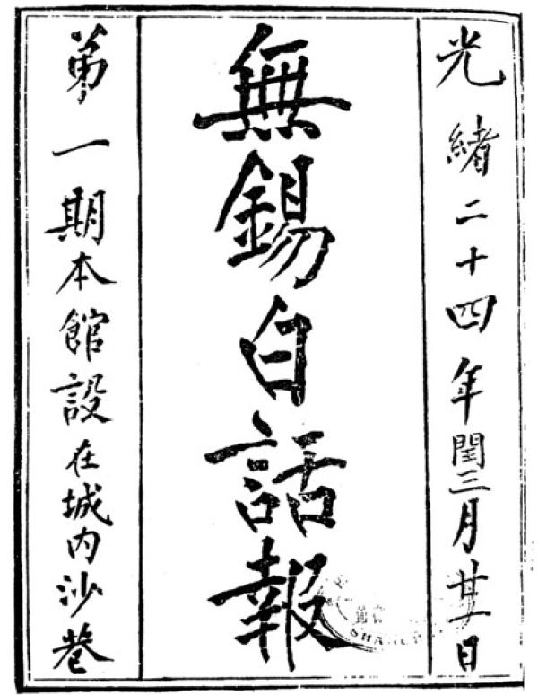
Wuxi Vernacular Newspaper, No.1, 1898
1898 was an "eventful autumn". Apart from the "Reform Movement of 1898" that shook the Qing court, the ups and downs of literary criticism in the press and literary circles all moved with the "great change in a hundred years". Countless intellectuals devoted themselves to the cause of "enlightening the foolish and enlightening the people’s wisdom". Among the numerous newspapers and magazines in the late Qing Dynasty and the early Republic of China, vernacular newspapers and periodicals are naturally a striking part. The fermentation and germination of all kinds of new and old ideological trends are extremely unstable and full of contingency. Various vernacular newspapers and periodicals established for the purpose of "enlightening the foolish" and vernacular chapters published in major newspapers and periodicals have played a catalytic role in this process, awakening modern women’s consciousness and shaping the image of "new women". Also in 1898, Wuxi Vernacular Newspaper(Later renamed China Guanyin Vernacular Newspaper)It was founded in Wuxi on May 11th, and the Journal of Women was founded in Shanghai on July 24th. The two newspapers are directly related to the practice of women’s vernacular and the prosperity of women’s studies. Although the editor-in-chief of Wuxi Vernacular Newspaper is Qiu Tingliang, the most important editor-in-chief is actually his niece Qiu Yufang. As an influential vernacular newspaper in the late Qing Dynasty, the newspaper content of Wuxi Vernacular Newspaper presents a complicated scene of literary and vernacular transformation. Qiu Yufang hesitated in the statute of women’s education, and her vernacular practice such as Notes on Women’s Commandments and Chronicle of Mencius became a microcosm of the germination of women’s consciousness in the late Qing Dynasty. As the journal of China Women’s Association, Journal of Women aims at promoting women’s studies and restoring women’s rights, and its words are easy to understand. The main contributors include Kang Tongwei, Xue Shaohui, Shen Heqing, Qiu Yufang, Li Huixian, Pan Xuan, Jiang Yufang and others, and there are as many as 18 main writers listed in the first issue alone. Women’s vernacular practice in newspapers and periodicals became an organic part of vernacular newspapers in the late Qing Dynasty.
There are countless reports about women in vernacular newspapers, including-first, news about the opening, enrollment and teaching of women’s schools, Anhui Vernacular Newspaper, National Vernacular Daily, Hangzhou Vernacular Newspaper, Shaoxing Vernacular Newspaper, Jilin Vernacular Newspaper and Zhili Vernacular Newspaper, etc., which have been reported many times, and some of them are "news of this province (local port)" Secondly, regarding the complex connection between women’s schools and the society in the late Qing Dynasty, the content of the debate started from schools, textbooks and students’ birth, and the concern for female students often combined with the general discussion of women in the late Qing Dynasty, that is, the re-transformation of the gender concept of the whole society. For example, the social news that prostitutes pretend to be female students published in Tianjin Vernacular Newspaper, and the satirical ditty published by Zhang Danfu in Jingye Xunbao, etc. There are also discussions on a series of social phenomena around women, such as women’s moral cultivation, freedom to get married, etc. For example, the National Opinion serialized by China Vernacular Newspaper has a special issue to discuss "women’s society", the editorials "Vulgar Articles" and "Re-discussing Marriage" serialized by Anhui Vernacular Newspaper, and the New Testament on Marriage serialized by Hangzhou Vernacular Newspaper, etc. Third, the initiative of calling on women to fight for their own rights and interests, actively enter school and be self-reliant is more inclined to the discourse of political power.For example, the long editorial "On Women’s Right to Restore Women’s Rights" serialized in National Vernacular Newspaper, and the speech "Wake Up Women Compatriots" published in Guangdong Vernacular Newspaper, etc. These vernacular newspapers either focus on women’s studies in the form of editorials and news reports, or promote new women in literary forms such as poems, operas and novels, and at the same time echo other vernacular works related to women in the late Qing Dynasty. In a word, the relevant vernacular newspapers in the late Qing Dynasty formed a dense communication network centered on the germination of female consciousness. The base camp of vernacular newspapers in the late Qing Dynasty was of course large and small vernacular newspapers, but at the same time, many newspapers that paid equal attention to both literature and vulgarity also set up columns such as "forum", "performance altar" and "speech" to publish articles written in vernacular or shallow classical Chinese. Most of these articles are vernacular speeches, that is, speeches written in the form of vernacular Chinese, which can be said to be recorded in a popular written language that simulates spoken language for people to read or for journalists to play. When the author writes, he imagines that he is a virtual journalist, such as the column "Playing the altar" in Women’s World, China Women’s Newspaper and China New Women’s Magazine. There are also some vernacular songs published in classical Chinese newspapers to promote women’s studies, oppose foot-binding and encourage female workers, which have certain artistic appeal, such as the song of kicking off feet in Chinese and Western Church Newspaper, the song of encouraging students published in the newspaper of Reply, and the collection of songs in Women’s World. Although this part of the vernacular newspapers published in classical Chinese newspapers are scattered everywhere, the number is very considerable.
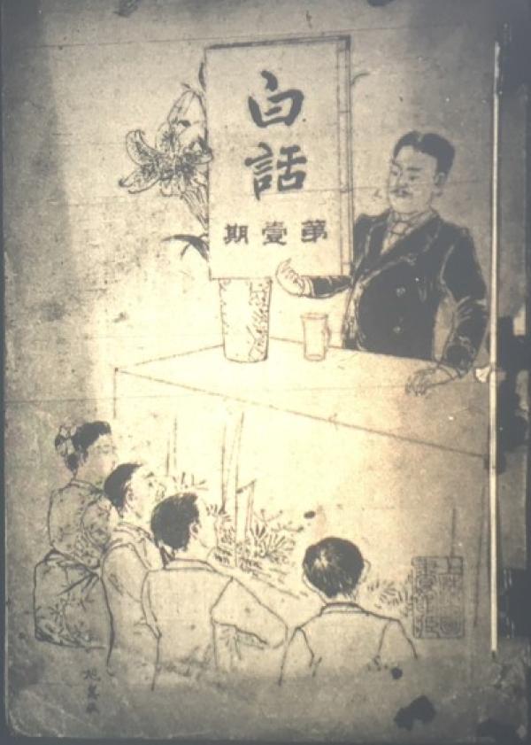
Vernacular, the first issue in 1904, was founded by Qiu Jin.
As early as before the May Fourth Vernacular Movement, Huang Zunxian’s "I wrote my mouth by hand, how can I be detained in ancient times?"("Miscellaneous feelings")Chen Rongqi’s "There is no elegance and vulgarity in speech"(As the saying goes)Qiu Tingliang’s "Advocating Vernacular and Abandoning Classical Chinese"("On Vernacular Language as the Foundation of Reform")And so on have put forward the idea of consistency in words and words. It is true that, as Zhou Zuoren pointed out, the vernacular and classical Chinese at that time were used by the "valet" and the "master" respectively, and many vernacular Chinese had a strong stereotype. Even the pioneers of vernacular Chinese such as Huang Zunxian, whose works promoting vernacular Chinese are mostly written in ancient poems and classical Chinese. However, from the objective effect, the vernacular practice of the vernacular movement in the late Qing Dynasty became the forerunner of the May 4th vernacular movement to some extent, which not only gave birth to writers and readers of vernacular, promoted vernacular teaching, affected the transformation process of China literature, but also provided the soil for the evolution of Chinese’s gender consciousness when the west wind spread eastward. It is worth noting that the female intellectuals in China in the late Qing Dynasty and the early Republic of China were not only active practitioners of vernacular writing, but also did not blindly follow suit in theoretical advocacy. According to Professor Xia Xiaohong’s research, in the inaugural issue of Shanghai Journal for Women on July 24th, 1898, Pan Xuan’s article "The Origin of Shanghai Journal for Women" has discriminated the dichotomy of classical Chinese, and put forward the idea of trying to figure out practical learning in vernacular Chinese, which was more than a month earlier than Qiu Tingliang’s proposal that "vernacular Chinese is the foundation of reform", and Qiu Yufang, the niece of the latter, also participated in the Journal for Women. The vernacular movement in the late Qing Dynasty and the awakening of modern women’s consciousness are in one vein. Although it is different from the May 4th Movement in terms of distinctiveness and determination, women’s expression in this period has its own tenacity and endurance.
The female expression in the transformation of literary Chinese is not only reflected in the changes of text practice such as style, vocabulary and grammatical structure, but also in the innovation of composition conception and writing concept, which is an important link in the construction of gender subject. A close look at the "discipline" of literary rhetoric in the vernacular newspaper corpus on discourse practice and the "delay" and "breakthrough" of women in literary expression can enrich and refine the modern gender subject research. At the same time, the literary language from the late Qing Dynasty to the May 4th Movement is intrinsically related to the pursuit of modernity, and language has formed an inseparable relationship chain with national salvation, enlightenment and prosperity. In this process, the awakening and maturity of women’s consciousness is closely related to language change and national crisis, and the prominence of modern gender subject is always accompanied by the birth of language subject and national subject.
During the nearly 20 years from the Vernacular Movement in the late Qing Dynasty to the Vernacular Movement in the May 4th Movement, with the deepening of the Chinese Pinyin Movement, various attempts to "speak and write the same" and "unify the language" were reflected in the historical ups and downs of the transformation of the vernacular. A group of scholars in the late Qing Dynasty tried to promote mass enlightenment through language reform. The transformation of literary Chinese in the late Qing Dynasty and the early Republic of China was accompanied by the rise of modern nationalism. On the road of modernization, the "differences" between Chinese and Western cultures were mostly classified as "gaps", and the "weakness" of China’s language and writing became the "shame" of Chinese people’s "courage after knowing shame". The strokes of Chinese characters are complicated and difficult, and learning to recite them is not as convenient as pinyin; The pronunciation of Chinese characters is not unified, and the spread of Chinese can only rely on classical Chinese. As a mature written language system, the communication ability of classical Chinese is limited, and there are obstacles in absorbing new theories. In the case of dichotomy of language and literature, people’s educational enlightenment is limited everywhere, and people’s hearts are scattered, so it is impossible to cultivate "new citizens", let alone resist foreign aggression. Under this deduction, the problem of language and writing eventually becomes the problem of preserving species in a powerful country. The rise of vernacular status is not only a cultural event, but also a political behavior of Chinese after several choices in the process of modernization. In the two clues of the vernacular movement and the Chinese Pinyin movement, the admiration and tempering of vernacular, the secondary processing of spoken language and the creative use of dialect vocabulary have become the joint points connecting literary language and women. For women at that time, on the one hand, the Qing government did not bring women’s studies into the official academic system until 1907,On the other hand, the practice of women’s discourse, including women’s education, women’s enlightenment and many other social issues, has long been seen in newspapers, and the teaching of women’s studies began in the 1840s. In the dual vision of language, culture and gender awareness, neologisms are intertwined with new styles, oral expression strategies and gender reference under the academic system, which refines the macro discussion of home and country into specific and subtle lines:
First, the new vocabulary and new style in the late Qing Dynasty from the perspective of female enlightenment. New terms such as "women’s rights", "women" and "female students" have become hot topics in the process of western learning spreading to the east, and their meanings have been localized with the interpretation of different literary forms such as novels, ballads and contemporary tunes, which have become an indispensable part of female enlightenment. The process of introducing new terms related to women is a process of translation and learning physics and chemistry; The borrowing of these new terms in the transformation of various literary styles is a process of enlightenment and popularization. The coupling and dislocation of the meanings of various new words in the two processes reflects the expectations of different groups for "new women".
Second, dialect, spoken language, vernacular and female expression strategies. Whether it’s political papers and speeches for women, school songs and novels, etc., we can increase the semantic interval, soften the tone, and narrow and imagine the distance between readers through written direct recording of dialects and spoken language. The direct written records of spoken language and dialects, such as "Du" and "Ge" in Wu dialect and "La", "Wu" and "Xi" in Cantonese, make the form of early vernacular literature more lively. However, the colloquial dialogues of female narrators are different in different works, and sometimes the written language and even classical Chinese components increase significantly. At this time, women can’t give up "classical Chinese" and the discourse authority behind it.
Thirdly, female text reference under the influence of female school system and female education statute. Works with women as narrators and texts with women as narrative objects use different pronouns for "I" and "she", such as "woman", "woman" and "sister", which reflects the conflict, transition and integration between traditional women’s education and westernized women’s studies in modern times, and gradually establishes the gender subject in the process of reference transformation. The teaching materials and writing paradigms involved in women’s schools in the late Qing Dynasty and the early Republic of China are interrelated with the singular and plural forms of references such as "women and children", "sisters" and "I (we)" in women’s text practice. China women awakened by the propaganda of "collective/individual" and "country/home" also experienced changes in words, genres and concepts in the process of composition.
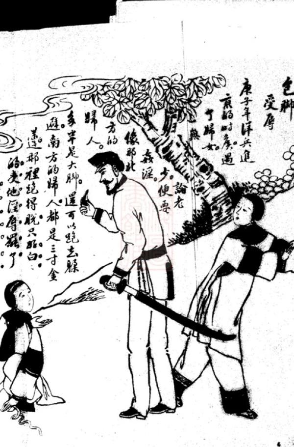
Picture of foot-wrapped humiliation, Anhui Daily, No.13, 1904.
What needs to be clear is that when discussing women’s writing, especially in the process of writing language changing from classical Chinese to vernacular Chinese, the opposition of gender identity cannot be simply linked with the opposition of classical Chinese and vernacular Chinese. If we can’t restore the context in combination with the scene of literary production, we can’t explain how some female vocalists continue the "discourse authority" of classical Chinese in their vernacular creation, nor can we explain the phenomenon that men use female pseudonyms, imitate women’s tone and call for women’s unity in their vernacular creation. However, since there is an attempt to imitate women’s tone writing, it means that there is at least a paradigm of women’s writing style, which is not a gender bias that needs to be broken, but a characteristic of women’s language in the historical context at that time. On the relationship between language and gender differences, many discussions in linguistics are quite enlightening. As early as 1922, Otto Jespersen wrote in his linguistic treatise The Essence, Development and Origin of Language (Language: its nature, development and origin) has devoted a special chapter to the characteristics of women’s language, and made a simple comparison between the language habits of the two sexes from the aspects of language taboos, vocabulary selection, grammar and sentence patterns. However, due to the limitations of the times, the author failed to provide systematic data support, but analyzed the reasons for the differences from the perspective of anthropology. Jesper’s view belongs to the typical "defect theory", that is, women’s language is a defective low-level version compared with men’s because of their limited education and most of them have not left home or engaged in labor production outside the family. With the development of linguistics and the influence of the western women’s movement, the discussion on language and gender differences since 1960s has successively produced two viewpoints, namely "dominance theory" and "difference theory".Language and Women’s Place, 1975) thinks that the language difference between men and women is the mapping of gender inequality in society, while the latter has emerged since the 1990s, and scholars represented by Alice R Freed began to correct the inappropriate exposition of men and women in the "defect theory" and "dominance theory". Different from previous studies, which regard women as passive roles, the "difference theorists" believe that both sexes have their own characteristics, and there is no distinction between higher and lower languages, and they are all equal individuals. It is not difficult to find that the western research on the relationship between gender and language is updated with the deepening of western women’s self-cognition. Although the viewpoints involved are rooted in the historical soil of western civilization, the discussion on women’s education, class, spoken and written language and discourse power is of great significance for reviewing and analyzing the transformation of women’s creative language in modern China.
In the process of the west spreading to the east, it is impossible for women in China to stay out of it, but their "voice" has to be torn with the women’s education regulations, and the women’s education regulations have changed because of the influence of the western education system on women’s education in China. The factors related to gender in the transitional period are no longer "constants". Therefore, it is necessary to fully consider the differences between Chinese and western women’s text practice, gender subject generation and feminist movement process, and firmly grasp the main clues of the evolution of modern China’s language and writing concepts in the collision and interweaving of tradition and modernity, and East and West. Only in this way can we establish a three-dimensional structure of literature, Chinese, women’s expression, country and nation through vertical and horizontal comparison, just like finding a criterion in the ubiquitous "variable" wrestling field in the literary production field.
(Part of this article comes from the online lecture "Women’s Expression in the Transition of Literariness in the Late Qing Dynasty and the Early Republic of China" given by the author to the Confucius Institute in Hong Kong and the China Department of Culture of the Hong Kong Polytechnic University on April 6th. )